|
|
|
|
|
|
Peer reviewed journals
61. Z. Qiao, Z. Yuan, S. Zhu, C. Gong, Y. Liao, X. Gong, M. Kim, D. Zhang, Y.-C. Chen*, "High orbital angular momentum lasing with tunable degree of chirality in a symmetry-broken microcavity", Optica, 10(7), 846 (2023).
60. Z. Wang, G. Fang*, Z. Gao, Y. Liao, C. Gong, M. Kim, G.-E. Chang, S. Feng, T. Xu, T. Liu, Y.-C. Chen*, "Autonomous microlasers for profiling extracellular vesicles from cancer spheroids", Nano Letters, 23(7), 2502 (2023). PDF
59. Y. Liao, Y. J. Kim, J. Lai, J.-H. Seo, M. Kim*, "Antireflective GaN Nanoridge Texturing by Metal-Assisted Chemical Etching via a Thermally Dewetted Pt Catalyst Network for Highly Responsive Ultraviolet Photodiodes", ACS Applied Materials & Interfaces, 15(10), 13343 (2023). PDF
58. B. Son, S.‐H. Shin, Z.‐J. Zhao, B.‐K. Ju, J.‐H. Jeong, M. Kim*, C. S. Tan, "High‐Efficiency Silicon Nanowire Array Near Infrared Photodetectors via Length Control and SiOx Surface Passivation", Advanced Materials Technologies, 2301131 (2023). PDF
57. Y.-C. Tai, S. An, P.-R. Huang, Y.-T. Jheng, K.-C. Lee, H.-H. Cheng, M. Kim*, G.-E. Chang*, "Transfer-printing-enabled GeSn flexible resonant-cavity-enhanced photodetectors with strain-amplified mid-infrared optical responses", Nanoscale, 15(17), 7745 (2023). PDF
56. Y. J. Kim, S. An, Y. Liao, P.-R. Huang, B. Son, C. S. Tan, G.-E. Chang, M. Kim*, "Flexible TiN/Ge photodetectors with enhanced responsivity via localized surface plasmon resonance and strain modulation", Journal of Materials Chemistry C, 11(13), 4520 (2023). PDF
55. A. Shu, H. Park, M. Kim*, "Recent advances in single crystalline narrow band-gap semiconductor nanomembranes and their flexible optoelectronic device applications: Ge, GeSn, InGaAs, and 2D materials", Journal of Materials Chemistry C, 11, 2430 (2023). PDF
54. H. Park, J. Kim, D. Choi, S.-W. Lee, D. Kang, H.-S. Lee, D. Kim, M. Kim*, Y. Kang*, "Boron‐doped polysilicon using spin‐on doping for high‐efficiency both‐side passivating contact silicon solar cells", Progress in Photovoltaics: Research and Applications, 31(5), 461 (2023). PDF
53. S. An, Y.-C. Huang, C.-Y. Wu. Qiao, P.-R. Huang, G.-E. Chang, J. Lai, J-H. Seo, M. Kim*, "Single‐Crystalline Ge1−xSnx/Si p–n Heterojunction Photodiodes with Sn Compositions up to 10%", Advanced Materials Technologies, 2201136 (2023). PDF
52. K. K. Chan, L.-Y. Shang, Z. Qiao, Y. Liao, M. Kim, Y.-C. Chen*, "Monitoring Amyloidogenesis with a 3D Deep-Learning-Guided Biolaser Imaging Array", Nano Letters, 22, 8949 (2022). PDF
51. Z. Yuan, S.-H. Huang, Z. Qiao, C. Gong, Y. Liao, M. Kim, M. D. Birowosuto, C. Dang, P. C. Wu*, Y.-C. Chen*, "Direct Imaging of Weak‐to‐Strong‐Coupling Dynamics in Biological Plasmon–Exciton Systems", Laser & Photonics Reviews, 2200016 (2022). PDF
50. Y. Liao, Y. Zheng, S.-H. Shin, Z.-J. Zhao, S. An, J.-H. Seo, J.-H. Jeong, and M. Kim*, "Distinct UV–Visible Responsivity Enhancement of GaAs Photodetectors via Monolithic Integration of Antireflective Nanopillar Structure and UV Absorbing IGZO Layer", Advanced Optical Materials, 2200062 (2022). PDF
49. B. Son, S.-H. Shin, Y. Jin, Y. Liao, Z.-J. Zhao, J.-H. Jeong, Q. J. Wang, X. Wang, C. S. Tan*, and M. Kim*, "A heavily doped germanium pyramid array for tunable optical antireflection in the broadband mid-infrared range", Journal of Materials Chemistry C, 10(15), 5797 (2022). - This article has been featured as a cover image of the journal. PDF
48. Y. Liao, S.-H. Shin, and M. Kim*, “Ultraviolet Antireflective Porous Nanoscale Periodic Hole Array of 4H-SiC by Photon-Enhanced Metal-Assisted Chemical Etching”, Applied Surface Science, 152387 (2022). PDF
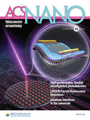
47. Z.-J. Zhao, S.-H. Shin, S. Y. Lee, B. Son, Y. Liao, S. Hwang, S. Jeon, H. Kang, M. Kim*, and J.-H Jeong*, “Direct Chemisorption-Assisted Nanotransfer Printing with Wafer-Scale Uniformity and Controllability”, ACS Nano, 16, 378 (2022). PDF
46. X. Gong, Z. Qiao, Y. Liao, S. Zhu, L. Shi, M. Kim, and Y.-C. Chen*, “Enzyme‐Programmable Microgel Lasers for Information Encoding and Anticounterfeiting”, Advanced Materials, 2107809 (2022). PDF
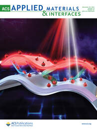
45. S. An, Y. Liao, and M. Kim*, “Flexible Titanium Nitride/Germanium-Tin Photodetectors Based on Sub-Bandgap Absorption”, ACS Applied Materials & Interfaces, 13, 61396 (2021). - This article has been featured as a cover image of the journal. PDF
44. Z. Qiao, C. Gong, Y. Liao, C. Wang, K.-K. Chan, S. Zhu, M. Kim, and Y.-C. Chen*, “Tunable Optical Vortex from a Nanogroove-Structured Optofluidic Microlaser”, Nano Letters, 22, 1425 (2021). PDF
43. Y.-Y. Zhang, S. An, Y. Zheng, J. Lai, J.-H. Seo, K. H. Lee, M. Kim*, “Releasable AlGaN/GaN 2D Electron Gas Heterostructure Membranes for Flexible Wide‐Bandgap Electronics”, Advanced Electronic Materials, 2100652 (2021). PDF
42. Q. Chen, Z. Wang, Z. Song, W. Fan*, K. Wang, M. Kim, and D. Zhang*, “Effect of thickness on the electronic structure and optical properties of quasi two-dimensional perovskite CsPbBr3 nanoplatelets”, Journal of Luminescence, 239, 118392 (2021). PDF
41. Y. Liao, S. H. Shin, Y. Jin, Q. J. Wang, and M. Kim*, “Producing Microscale Ge Textures via Titanium Nitride- and Nickel-Assisted Chemical Etching with CMOS-Compatibility”, Advanced Materials Interfaces, 2100937 (2021). PDF
40. S. An, Y. Liao, and M. Kim*, “Black Germanium Photodetector Exceeds External Quantum Efficiency of 160%”, Advanced Materials Technologies, 2100912 (2021). - This article has been exclusively featured by Nature Electronics. PDF PDF2
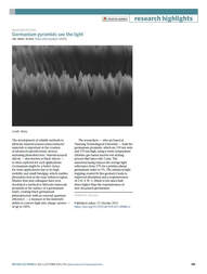
39. S.-H. Shin, Y. Liao, B. Son, Z. Zhao, J.-H. Jeong, C. S. Tan, and M. Kim*, "Highly Ordered and Damage-Free Ge Inverted Pyramid Array Structure for Broadband Antireflection in the Mid-Infrared", Journal of Materials Chemistry C, 9, 9884 (2021). - This article has been featured as a cover image of the journal. PDF
38. Y. Hwang, A. Sadhu, S. Shin, S. W. Leow, Z. Zhao, J. Deng, J. A. Jackman, M. Kim, L. H. Wong*, and N.-J. Cho*, “Intrinsically micro/nano-structured pollen substrate with tunable optical properties for optoelectronic applications”, Advanced Materials, 2100566 (2021). PDF
37. J. A. Michaels, L. Janavicius, X. Wu, C. Chan, H.-H. Huang, S. Namiki, M. Kim, D. Sievers, and X. Li*, “Producing Silicon Carbide Micro and Nanostructures by Plasma-free Metal-Assisted Chemical Etching”, Advanced Functional Materials, 2103298 (2021). PDF
36. S. An, Y.-C. Tai, K.-C. Lee, S. H. Shin, H. H. Cheng, G.-E. Chang*, and M. Kim*, “Raman scattering study of GeSn under <1 0 0> and <1 1 0> uniaxial stress”, Nanotechnology, 32(35), 355704 (2021). PDF
35. Y.-Y. Zhang, Y.-X. Zheng, J.-Y. Lai, J.-H. Seo, K. H. Lee, C. S. Tan, S. An, S.-H. Shin, B. Son, and M. Kim*, “High Performance Flexible Visible-Blind Ultraviolet Photodetectors with Two-Dimensional Electron Gas Based on Unconventional Release Strategy”, ACS Nano, 15(5), 8386-8396 (2021). - This article has been featured as an front cover of the journal and highlighted by NTU media coverage and major news outlets. PDF
34. S. An, S. Wu, K.-H. Lee, C. S. Tan, Y.-C. Tai, G.-E. Chang, and M. Kim*, “High-Sensitivity and Mechanically Compliant Flexible Ge Photodetectors with a Vertical p–i–n Configuration”, ACS Applied Electronic Materials, 3(4), 1780 (2021). PDF
33. Y.-Y. Zhang, S.-H. Shin, H.-J. Kang, S. Jeon, S. H. Hwang, W. Zhou, J-H. Jeong, X. Li, and M. Kim*, “Anti-reflective porous Ge by open-circuit and lithography-free metal-assisted chemical etching”, Applied Surface Science, 546, 149083 (2021). PDF
32. Z. Qiao, X. Gong, P. Guan, Z. Yuan, S. Feng, Y. Zhang, M. Kim, G.-E. Chang, and Y.-C. Chen*, “Lasing action in microdroplets modulated by interfacial molecular forces”, Advanced Photonics, 3(1), 016003 (2021). PDF
31. J. Lai, M. N. Hassan, E. Swinnich, Z. Tang, S.-H. Shin, M. Kim, P. Zhang, and J.-H. Seo*, "Flexible crystalline β-Ga2O3 solar-blind photodetectors", Journal of Materials Chemistry C, 8(42), 14732 (2020). Featured as an back cover. PDF
30. S. An, S. Wu, C. S. Tan, G-E. Chang, X. Gong, and M. Kim*, "Modulation of light absorption in flexible GeSn metal–semiconductor–metal photodetectors by mechanical bending", Journal of Materials Chemistry C, 8, 13557-13562 (2020). *Corresponding Featured as an front outside cover. PDF
29. S. Ghosh, K.-C. Lin, C.-S, Tsai, H. Kumar, Q. Chen, L. Zhang, B. Son, C. S. Tan, M. Kim, B. Mukhopadhyay, and G.-E. Chang*, "Metal-Semiconductor-Metal GeSn Photodetectors on Silicon for Short-Wave Infrared Applications", Micromachines, 11(9), pp. 795 (2020). PDF
28. Y.-C. Tai, P.-L. Yeh, S. An, H.-H. Cheng, M. Kim*, and G.-E. Chang*, "Strain-free GeSn nanomembranes enabled by transfer-printing techniques for advanced optoelectronic applications", Nanotechnology, 31(44), pp. 445301 (2020). *Corresponding PDF
27. J.-H. Seo*, E. Swinnich, Y.-Y. Zhang, and M. Kim*, "Low dimensional freestanding semiconductors for flexible optoelectronics: materials, synthesis, process, and applications", Materials Research Letters, (Invited review) 8(4), pp. 123-144 (2020). *Corresponding PDF
26. J. D. Kim**, M. Kim**, C. Chan, N. Draeger, J. Coleman, and X. Li*, "CMOS Compatible Catalyst for MacEtch: Titanium Nitride Assisted Chemical Etching in Vapor Phase for High Aspect Ratio Silicon Nanostructures", ACS Applied Materials & Interfaces, 11(30), pp. 27371-27377 (2019). **equal contribution PDF
25. H.-C. Huang**, M. Kim**, X. Zhan, K. Chabak, J. D. Kim, A. Kvit, D. Liu, Z. Ma, J.-M. Zuo, and X, Li*, "High Aspect Ratio β-Ga2O3 Fin Arrays with Low Interface Charge Density by Inverse Metal-Assisted Chemical Etching", ACS Nano, 13(8), pp. 8784-8792 (2019). **equal contribution PDF
24. S. J. Cho, D. Liu, J.-H. Seo, R. Dalmau, K. Kim, J. Park, J. Gong, D. Zhao, F. Wang, X. Yin, Y. H. Jung, I.-K. Lee, M. Kim, X. Wang, J. D. Albrecht, W. Zhou, B. Moody, and Z. Ma*, "P-type silicon as hole supplier for nitride-based UVC LEDs", New Journal of Physics, 21, 023011 (2019). PDF
23. M. Kim, H. C. Hwang, J. D. Kim, K. D. Chabak, ARK Kalapala, W. Zhou, and X. Li*, “Nanoscale groove textured β-Ga2O3 by room temperature inverse metal-assisted chemical etching and photodiodes with enhanced responsivity”, Applied Physics Letters, 113, 222104 (2018). PDF
After joining NTU
22. D. Liu, S. J. Cho, J. Park, J. Gong, J.-H. Seo, R. Dalmau, D. Zhao, K. Kim, M. Kim, ARK Kalapala, J. D. Albrecht, W. Zhou, B. Moody, and Z. Ma, “226 nm AlGaN/AlN UV LEDs using p-type Si for hole injection and UV reflection”, Applied Physics Letters, 113, 011111 (2018).
21. M. Kim, S. Yi, J. D. Kim, X. Yin, J. Li, J. Bong, D. Liu, S.-C. Liu, A. Kvit, W. Zhou, X. Wang, Z. Yu, Z. Ma, and X. Li, “Enhanced Performance of Ge Photodiodes via Monolithic Antireflection Texturing and α-Ge Self-Passivation by Inverse Metal-Assisted Chemical Etching”, ACS Nano, 12(7), pp. 6748-6755 (2018).
20. J. D. Kim*, M. Kim*, L. Kong, P. Mohseni, S. Ranganathan, J. Pachamuthu, W. K. Chim, S. Y. Chiam, J. Coleman, and X. Li, “Self-Anchored Catalyst Interface Enables Ordered Via Array Formation from Submicrometer to Millimeter Scale For Polycrystalline and Single-Crystalline Silicon”, ACS Applied Materials & Interfaces, 10(10), pp. 9116-9122 (2018). *equal contribution
19. D. Liu, S. J. Cho, J. Park, J.-H. Seo, R. Dalmau, D. Zhao, K. Kim, J. Gong, M. Kim, I.-K. Lee, J. D. Albrecht, W. Zhou, B. Moody, and Z. Ma, “229 nm UV LEDs on aluminum nitride single crystal substrates using p-type silicon for increased hole injection”, Applied Physics Letters, 112, 081101 (2018).
18. M. Kim, S. J. Cho, Y. J. Dave, H. Mi, S. Mikael, J.-H. Seo, J. U. Yoon, Z. Ma, “Fabrication of Ge on insulator wafers by Smart-CutTM with thermal management for undamaged donor Ge wafers”, Semiconductor Science Technology, 33, 015017 (2018).
17. K. Zhang, Y. H. Jung, S. Mikael, J.-H. Seo, M. Kim, H. Mi, H. Zhou, Z. Xia, W. Zhou, S. Gong, and Z. Ma, “Origami Silicon Optoelectronics for Hemispherical Electronic Eye Systems”, Nature Communications, 8, 1782 (2017).
16. J.-H. Seo, K. Zhang, M. Kim, W. Zhou Z. Ma, “High-Performance Flexible BiCMOS Electronics Based on Single-Crystal Si Nanomembrane”, npj Flexible Electronics, 1, pp. 1-7 (2017).
15. M. Kim, J.-H. Seo, U. Singisetti, and Z. Ma, “Recent advances in free-standing single crystalline wide band-gap semiconductors and their applications: GaN, SiC, ZnO, β-Ga2O3, and diamond”, Journal of Materials Chemistry C, (Invited Review) 5, pp. 8338-8354 (2017). – This article has been featured as an outside back cover of the journal.
14. Z. Xia*, H. Song*, M. Kim*, M. Zhou, T.-H. Chang, D. Liu, X. Yin, K. Xiong, H. Mi, X. Wang, F. Xia, Z. Yu, Z. Ma, and Q. Gan, “Single-crystalline Germanium nanomembrane photodetectors on foreign nanocavities”, Science Advances, 3(7), e1602783 (2017). *equal contribution – This article has been highlighted in Science Daily, Laser Focus World, Phys.Org, and more.
13. M. Kim, J.-H. Seo, D. Zhao, S.-C. Liu, K. Kim, W. Zhou, E. Waks, and Z. Ma, “Transferrable single crystalline 4H-SiC nanomembranes”, Journal of Materials Chemistry C, 5(2), pp. 264-268 (2017). – This article has been selected as 2016 Journal of Materials Chemistry C Hot Paper and featured as an inside front cover of the journal and on the main pages of engr.wsic.edu.
12. S. Mikael, J.-H. Seo, D.-W. Park, M. Kim, H. Mi, S. Gong, Z. Ma, "Triaxial Strain in Bilayer Graphene Enabled by the Nitride Stressor Layer", Extreme Mechanics Letters, 11, pp. 77-83 (2017).
11. M. Kim, J.-H. Seo, Z. Yu, W. Zhou Z. Ma, “Flexible Germanium Nanomembrane Metal Semiconductor-Metal (MSM) photodiodes”, Applied Physics Letters, 109, 051105 (2016). - This article has been selected as an Editor’s pick article.
10. M. Kim, S.-C. Liu, T. J. Kim, J. Lee, J.-H. Seo, W. Zhou, Z. Ma, “Light absorption enhancement in Ge nanomembrane and its optoelectronic application”, Optics Express, 24, 15, 16894-16903 (2016).
9. M. Cho, J.-H. Seo, M. Kim, J. Lee, D. Liu, W. Zhou, Z. Yu, Z. Ma, “Resonant cavity (RC) germanium photodetector via stacked single-crystalline nanomembranes”, Journal of Vacuum Science and Technology B 34, 040604 (2016).
8. M. Cho, J.-H. Seo, D. Zhao, J. Lee, K. Xiong, X. Yin, Y. Liu, S.-C. Liu, M. Kim, T. Kim, X. Wang, W. Zhou, and Z. Ma, “Amorphous Si/SiO2 distributed Bragg reflectors with transfer printed single-crystalline Si nanomembranes”, Journal of Vacuum Science and Technology B, 34, 040601 (2016). - This article has been selected as an Editor’s pick article.
7. J.-H. Seo, K. Zhang, M. Kim, H. Yang, W. Zhou, Z. Ma, “Flexible Phototransistors Based on Single Crystalline Silicon Nanomembranes”, Advanced Optical Materials, 4, 1 (2015). - This article has been featured as a front cover and highlighted in IEEE Spectrum, Phys.ORG, AAAS + more than 100 news worldwide.
6. Y. H. Jung, T.-H Chang, H. Zhang, C. Yao, Q. Zheng, V. W. Yang, H. Mi, M. Kim, S. J. Cho, D.-W. Park, H. Jiang, J. Lee, Y. Qiu, Z. Cai, W. Zhou, S. Gong, Z. Ma, “High-Performance Green Flexible Electronics Based on Biodegradable Cellulose Nanofibril Paper”, Nature Communications, 6, 7170 (2015). - This article has been featured on the main pages of wisc.edu, College of Engineering, Electrical and Computer Engineering, in addition to more than 100 news stories worldwide.
5. M. Kim, H. Mi, M. Cho, J.-H. Seo, W. Zhou, S. Gong, Z. Ma, “Tunable biaxial in-plane compressive strain in a Si nanomembrane transferred on a polyimide film”, Applied Physics Letters, 106, 212107 (2015).
4. M. Kim, W. Fan, J.-H. Seo, N. Cho, S. Liu, D. Geng, S. Gong, X. D Wang, W. Zhou, Z. Ma, “Polycrystalline GeSn thin film on Si formed by alloy evaporation”, Applied Physics Express, 8 061301 (2015).
3. M. Cho, J.-H. Seo, J. Lee, D. Zhao, H. Mi, X. Yin, M. Kim, X. Wang, W. Zhou, Z. Ma, “Ultra-thin distributed Bragg reflectors via stacked single-crystal silicon nanomembranes”, Applied Physics Letters, 106, 181107 (2015).
2. M. Kim, J. G. Yang, and K. Yang, “A Switched Transmission-Line Type Q-Band 4-Bit Phase Shifter Using InGaAs PIN Diodes”, IET Electronics Letters, Vol. 46, No. 3, pp. 219 -220 (2010).
1. M. Kim, J. G. Yang, and K. Yang, “High Performance Q-Band MMIC Phase Shifters Using InGaAs PIN Diodes”, J. Electromagn. Eng. Sci., vol. 9, no. 3, pp. 159-163 (2009).
61. Z. Qiao, Z. Yuan, S. Zhu, C. Gong, Y. Liao, X. Gong, M. Kim, D. Zhang, Y.-C. Chen*, "High orbital angular momentum lasing with tunable degree of chirality in a symmetry-broken microcavity", Optica, 10(7), 846 (2023).
60. Z. Wang, G. Fang*, Z. Gao, Y. Liao, C. Gong, M. Kim, G.-E. Chang, S. Feng, T. Xu, T. Liu, Y.-C. Chen*, "Autonomous microlasers for profiling extracellular vesicles from cancer spheroids", Nano Letters, 23(7), 2502 (2023). PDF
59. Y. Liao, Y. J. Kim, J. Lai, J.-H. Seo, M. Kim*, "Antireflective GaN Nanoridge Texturing by Metal-Assisted Chemical Etching via a Thermally Dewetted Pt Catalyst Network for Highly Responsive Ultraviolet Photodiodes", ACS Applied Materials & Interfaces, 15(10), 13343 (2023). PDF
58. B. Son, S.‐H. Shin, Z.‐J. Zhao, B.‐K. Ju, J.‐H. Jeong, M. Kim*, C. S. Tan, "High‐Efficiency Silicon Nanowire Array Near Infrared Photodetectors via Length Control and SiOx Surface Passivation", Advanced Materials Technologies, 2301131 (2023). PDF
57. Y.-C. Tai, S. An, P.-R. Huang, Y.-T. Jheng, K.-C. Lee, H.-H. Cheng, M. Kim*, G.-E. Chang*, "Transfer-printing-enabled GeSn flexible resonant-cavity-enhanced photodetectors with strain-amplified mid-infrared optical responses", Nanoscale, 15(17), 7745 (2023). PDF
56. Y. J. Kim, S. An, Y. Liao, P.-R. Huang, B. Son, C. S. Tan, G.-E. Chang, M. Kim*, "Flexible TiN/Ge photodetectors with enhanced responsivity via localized surface plasmon resonance and strain modulation", Journal of Materials Chemistry C, 11(13), 4520 (2023). PDF
55. A. Shu, H. Park, M. Kim*, "Recent advances in single crystalline narrow band-gap semiconductor nanomembranes and their flexible optoelectronic device applications: Ge, GeSn, InGaAs, and 2D materials", Journal of Materials Chemistry C, 11, 2430 (2023). PDF
54. H. Park, J. Kim, D. Choi, S.-W. Lee, D. Kang, H.-S. Lee, D. Kim, M. Kim*, Y. Kang*, "Boron‐doped polysilicon using spin‐on doping for high‐efficiency both‐side passivating contact silicon solar cells", Progress in Photovoltaics: Research and Applications, 31(5), 461 (2023). PDF
53. S. An, Y.-C. Huang, C.-Y. Wu. Qiao, P.-R. Huang, G.-E. Chang, J. Lai, J-H. Seo, M. Kim*, "Single‐Crystalline Ge1−xSnx/Si p–n Heterojunction Photodiodes with Sn Compositions up to 10%", Advanced Materials Technologies, 2201136 (2023). PDF
52. K. K. Chan, L.-Y. Shang, Z. Qiao, Y. Liao, M. Kim, Y.-C. Chen*, "Monitoring Amyloidogenesis with a 3D Deep-Learning-Guided Biolaser Imaging Array", Nano Letters, 22, 8949 (2022). PDF
51. Z. Yuan, S.-H. Huang, Z. Qiao, C. Gong, Y. Liao, M. Kim, M. D. Birowosuto, C. Dang, P. C. Wu*, Y.-C. Chen*, "Direct Imaging of Weak‐to‐Strong‐Coupling Dynamics in Biological Plasmon–Exciton Systems", Laser & Photonics Reviews, 2200016 (2022). PDF
50. Y. Liao, Y. Zheng, S.-H. Shin, Z.-J. Zhao, S. An, J.-H. Seo, J.-H. Jeong, and M. Kim*, "Distinct UV–Visible Responsivity Enhancement of GaAs Photodetectors via Monolithic Integration of Antireflective Nanopillar Structure and UV Absorbing IGZO Layer", Advanced Optical Materials, 2200062 (2022). PDF
49. B. Son, S.-H. Shin, Y. Jin, Y. Liao, Z.-J. Zhao, J.-H. Jeong, Q. J. Wang, X. Wang, C. S. Tan*, and M. Kim*, "A heavily doped germanium pyramid array for tunable optical antireflection in the broadband mid-infrared range", Journal of Materials Chemistry C, 10(15), 5797 (2022). - This article has been featured as a cover image of the journal. PDF
48. Y. Liao, S.-H. Shin, and M. Kim*, “Ultraviolet Antireflective Porous Nanoscale Periodic Hole Array of 4H-SiC by Photon-Enhanced Metal-Assisted Chemical Etching”, Applied Surface Science, 152387 (2022). PDF
47. Z.-J. Zhao, S.-H. Shin, S. Y. Lee, B. Son, Y. Liao, S. Hwang, S. Jeon, H. Kang, M. Kim*, and J.-H Jeong*, “Direct Chemisorption-Assisted Nanotransfer Printing with Wafer-Scale Uniformity and Controllability”, ACS Nano, 16, 378 (2022). PDF
46. X. Gong, Z. Qiao, Y. Liao, S. Zhu, L. Shi, M. Kim, and Y.-C. Chen*, “Enzyme‐Programmable Microgel Lasers for Information Encoding and Anticounterfeiting”, Advanced Materials, 2107809 (2022). PDF
45. S. An, Y. Liao, and M. Kim*, “Flexible Titanium Nitride/Germanium-Tin Photodetectors Based on Sub-Bandgap Absorption”, ACS Applied Materials & Interfaces, 13, 61396 (2021). - This article has been featured as a cover image of the journal. PDF
44. Z. Qiao, C. Gong, Y. Liao, C. Wang, K.-K. Chan, S. Zhu, M. Kim, and Y.-C. Chen*, “Tunable Optical Vortex from a Nanogroove-Structured Optofluidic Microlaser”, Nano Letters, 22, 1425 (2021). PDF
43. Y.-Y. Zhang, S. An, Y. Zheng, J. Lai, J.-H. Seo, K. H. Lee, M. Kim*, “Releasable AlGaN/GaN 2D Electron Gas Heterostructure Membranes for Flexible Wide‐Bandgap Electronics”, Advanced Electronic Materials, 2100652 (2021). PDF
42. Q. Chen, Z. Wang, Z. Song, W. Fan*, K. Wang, M. Kim, and D. Zhang*, “Effect of thickness on the electronic structure and optical properties of quasi two-dimensional perovskite CsPbBr3 nanoplatelets”, Journal of Luminescence, 239, 118392 (2021). PDF
41. Y. Liao, S. H. Shin, Y. Jin, Q. J. Wang, and M. Kim*, “Producing Microscale Ge Textures via Titanium Nitride- and Nickel-Assisted Chemical Etching with CMOS-Compatibility”, Advanced Materials Interfaces, 2100937 (2021). PDF
40. S. An, Y. Liao, and M. Kim*, “Black Germanium Photodetector Exceeds External Quantum Efficiency of 160%”, Advanced Materials Technologies, 2100912 (2021). - This article has been exclusively featured by Nature Electronics. PDF PDF2
39. S.-H. Shin, Y. Liao, B. Son, Z. Zhao, J.-H. Jeong, C. S. Tan, and M. Kim*, "Highly Ordered and Damage-Free Ge Inverted Pyramid Array Structure for Broadband Antireflection in the Mid-Infrared", Journal of Materials Chemistry C, 9, 9884 (2021). - This article has been featured as a cover image of the journal. PDF
38. Y. Hwang, A. Sadhu, S. Shin, S. W. Leow, Z. Zhao, J. Deng, J. A. Jackman, M. Kim, L. H. Wong*, and N.-J. Cho*, “Intrinsically micro/nano-structured pollen substrate with tunable optical properties for optoelectronic applications”, Advanced Materials, 2100566 (2021). PDF
37. J. A. Michaels, L. Janavicius, X. Wu, C. Chan, H.-H. Huang, S. Namiki, M. Kim, D. Sievers, and X. Li*, “Producing Silicon Carbide Micro and Nanostructures by Plasma-free Metal-Assisted Chemical Etching”, Advanced Functional Materials, 2103298 (2021). PDF
36. S. An, Y.-C. Tai, K.-C. Lee, S. H. Shin, H. H. Cheng, G.-E. Chang*, and M. Kim*, “Raman scattering study of GeSn under <1 0 0> and <1 1 0> uniaxial stress”, Nanotechnology, 32(35), 355704 (2021). PDF
35. Y.-Y. Zhang, Y.-X. Zheng, J.-Y. Lai, J.-H. Seo, K. H. Lee, C. S. Tan, S. An, S.-H. Shin, B. Son, and M. Kim*, “High Performance Flexible Visible-Blind Ultraviolet Photodetectors with Two-Dimensional Electron Gas Based on Unconventional Release Strategy”, ACS Nano, 15(5), 8386-8396 (2021). - This article has been featured as an front cover of the journal and highlighted by NTU media coverage and major news outlets. PDF
34. S. An, S. Wu, K.-H. Lee, C. S. Tan, Y.-C. Tai, G.-E. Chang, and M. Kim*, “High-Sensitivity and Mechanically Compliant Flexible Ge Photodetectors with a Vertical p–i–n Configuration”, ACS Applied Electronic Materials, 3(4), 1780 (2021). PDF
33. Y.-Y. Zhang, S.-H. Shin, H.-J. Kang, S. Jeon, S. H. Hwang, W. Zhou, J-H. Jeong, X. Li, and M. Kim*, “Anti-reflective porous Ge by open-circuit and lithography-free metal-assisted chemical etching”, Applied Surface Science, 546, 149083 (2021). PDF
32. Z. Qiao, X. Gong, P. Guan, Z. Yuan, S. Feng, Y. Zhang, M. Kim, G.-E. Chang, and Y.-C. Chen*, “Lasing action in microdroplets modulated by interfacial molecular forces”, Advanced Photonics, 3(1), 016003 (2021). PDF
31. J. Lai, M. N. Hassan, E. Swinnich, Z. Tang, S.-H. Shin, M. Kim, P. Zhang, and J.-H. Seo*, "Flexible crystalline β-Ga2O3 solar-blind photodetectors", Journal of Materials Chemistry C, 8(42), 14732 (2020). Featured as an back cover. PDF
30. S. An, S. Wu, C. S. Tan, G-E. Chang, X. Gong, and M. Kim*, "Modulation of light absorption in flexible GeSn metal–semiconductor–metal photodetectors by mechanical bending", Journal of Materials Chemistry C, 8, 13557-13562 (2020). *Corresponding Featured as an front outside cover. PDF
29. S. Ghosh, K.-C. Lin, C.-S, Tsai, H. Kumar, Q. Chen, L. Zhang, B. Son, C. S. Tan, M. Kim, B. Mukhopadhyay, and G.-E. Chang*, "Metal-Semiconductor-Metal GeSn Photodetectors on Silicon for Short-Wave Infrared Applications", Micromachines, 11(9), pp. 795 (2020). PDF
28. Y.-C. Tai, P.-L. Yeh, S. An, H.-H. Cheng, M. Kim*, and G.-E. Chang*, "Strain-free GeSn nanomembranes enabled by transfer-printing techniques for advanced optoelectronic applications", Nanotechnology, 31(44), pp. 445301 (2020). *Corresponding PDF
27. J.-H. Seo*, E. Swinnich, Y.-Y. Zhang, and M. Kim*, "Low dimensional freestanding semiconductors for flexible optoelectronics: materials, synthesis, process, and applications", Materials Research Letters, (Invited review) 8(4), pp. 123-144 (2020). *Corresponding PDF
26. J. D. Kim**, M. Kim**, C. Chan, N. Draeger, J. Coleman, and X. Li*, "CMOS Compatible Catalyst for MacEtch: Titanium Nitride Assisted Chemical Etching in Vapor Phase for High Aspect Ratio Silicon Nanostructures", ACS Applied Materials & Interfaces, 11(30), pp. 27371-27377 (2019). **equal contribution PDF
25. H.-C. Huang**, M. Kim**, X. Zhan, K. Chabak, J. D. Kim, A. Kvit, D. Liu, Z. Ma, J.-M. Zuo, and X, Li*, "High Aspect Ratio β-Ga2O3 Fin Arrays with Low Interface Charge Density by Inverse Metal-Assisted Chemical Etching", ACS Nano, 13(8), pp. 8784-8792 (2019). **equal contribution PDF
24. S. J. Cho, D. Liu, J.-H. Seo, R. Dalmau, K. Kim, J. Park, J. Gong, D. Zhao, F. Wang, X. Yin, Y. H. Jung, I.-K. Lee, M. Kim, X. Wang, J. D. Albrecht, W. Zhou, B. Moody, and Z. Ma*, "P-type silicon as hole supplier for nitride-based UVC LEDs", New Journal of Physics, 21, 023011 (2019). PDF
23. M. Kim, H. C. Hwang, J. D. Kim, K. D. Chabak, ARK Kalapala, W. Zhou, and X. Li*, “Nanoscale groove textured β-Ga2O3 by room temperature inverse metal-assisted chemical etching and photodiodes with enhanced responsivity”, Applied Physics Letters, 113, 222104 (2018). PDF
After joining NTU
22. D. Liu, S. J. Cho, J. Park, J. Gong, J.-H. Seo, R. Dalmau, D. Zhao, K. Kim, M. Kim, ARK Kalapala, J. D. Albrecht, W. Zhou, B. Moody, and Z. Ma, “226 nm AlGaN/AlN UV LEDs using p-type Si for hole injection and UV reflection”, Applied Physics Letters, 113, 011111 (2018).
21. M. Kim, S. Yi, J. D. Kim, X. Yin, J. Li, J. Bong, D. Liu, S.-C. Liu, A. Kvit, W. Zhou, X. Wang, Z. Yu, Z. Ma, and X. Li, “Enhanced Performance of Ge Photodiodes via Monolithic Antireflection Texturing and α-Ge Self-Passivation by Inverse Metal-Assisted Chemical Etching”, ACS Nano, 12(7), pp. 6748-6755 (2018).
20. J. D. Kim*, M. Kim*, L. Kong, P. Mohseni, S. Ranganathan, J. Pachamuthu, W. K. Chim, S. Y. Chiam, J. Coleman, and X. Li, “Self-Anchored Catalyst Interface Enables Ordered Via Array Formation from Submicrometer to Millimeter Scale For Polycrystalline and Single-Crystalline Silicon”, ACS Applied Materials & Interfaces, 10(10), pp. 9116-9122 (2018). *equal contribution
19. D. Liu, S. J. Cho, J. Park, J.-H. Seo, R. Dalmau, D. Zhao, K. Kim, J. Gong, M. Kim, I.-K. Lee, J. D. Albrecht, W. Zhou, B. Moody, and Z. Ma, “229 nm UV LEDs on aluminum nitride single crystal substrates using p-type silicon for increased hole injection”, Applied Physics Letters, 112, 081101 (2018).
18. M. Kim, S. J. Cho, Y. J. Dave, H. Mi, S. Mikael, J.-H. Seo, J. U. Yoon, Z. Ma, “Fabrication of Ge on insulator wafers by Smart-CutTM with thermal management for undamaged donor Ge wafers”, Semiconductor Science Technology, 33, 015017 (2018).
17. K. Zhang, Y. H. Jung, S. Mikael, J.-H. Seo, M. Kim, H. Mi, H. Zhou, Z. Xia, W. Zhou, S. Gong, and Z. Ma, “Origami Silicon Optoelectronics for Hemispherical Electronic Eye Systems”, Nature Communications, 8, 1782 (2017).
16. J.-H. Seo, K. Zhang, M. Kim, W. Zhou Z. Ma, “High-Performance Flexible BiCMOS Electronics Based on Single-Crystal Si Nanomembrane”, npj Flexible Electronics, 1, pp. 1-7 (2017).
15. M. Kim, J.-H. Seo, U. Singisetti, and Z. Ma, “Recent advances in free-standing single crystalline wide band-gap semiconductors and their applications: GaN, SiC, ZnO, β-Ga2O3, and diamond”, Journal of Materials Chemistry C, (Invited Review) 5, pp. 8338-8354 (2017). – This article has been featured as an outside back cover of the journal.
14. Z. Xia*, H. Song*, M. Kim*, M. Zhou, T.-H. Chang, D. Liu, X. Yin, K. Xiong, H. Mi, X. Wang, F. Xia, Z. Yu, Z. Ma, and Q. Gan, “Single-crystalline Germanium nanomembrane photodetectors on foreign nanocavities”, Science Advances, 3(7), e1602783 (2017). *equal contribution – This article has been highlighted in Science Daily, Laser Focus World, Phys.Org, and more.
13. M. Kim, J.-H. Seo, D. Zhao, S.-C. Liu, K. Kim, W. Zhou, E. Waks, and Z. Ma, “Transferrable single crystalline 4H-SiC nanomembranes”, Journal of Materials Chemistry C, 5(2), pp. 264-268 (2017). – This article has been selected as 2016 Journal of Materials Chemistry C Hot Paper and featured as an inside front cover of the journal and on the main pages of engr.wsic.edu.
12. S. Mikael, J.-H. Seo, D.-W. Park, M. Kim, H. Mi, S. Gong, Z. Ma, "Triaxial Strain in Bilayer Graphene Enabled by the Nitride Stressor Layer", Extreme Mechanics Letters, 11, pp. 77-83 (2017).
11. M. Kim, J.-H. Seo, Z. Yu, W. Zhou Z. Ma, “Flexible Germanium Nanomembrane Metal Semiconductor-Metal (MSM) photodiodes”, Applied Physics Letters, 109, 051105 (2016). - This article has been selected as an Editor’s pick article.
10. M. Kim, S.-C. Liu, T. J. Kim, J. Lee, J.-H. Seo, W. Zhou, Z. Ma, “Light absorption enhancement in Ge nanomembrane and its optoelectronic application”, Optics Express, 24, 15, 16894-16903 (2016).
9. M. Cho, J.-H. Seo, M. Kim, J. Lee, D. Liu, W. Zhou, Z. Yu, Z. Ma, “Resonant cavity (RC) germanium photodetector via stacked single-crystalline nanomembranes”, Journal of Vacuum Science and Technology B 34, 040604 (2016).
8. M. Cho, J.-H. Seo, D. Zhao, J. Lee, K. Xiong, X. Yin, Y. Liu, S.-C. Liu, M. Kim, T. Kim, X. Wang, W. Zhou, and Z. Ma, “Amorphous Si/SiO2 distributed Bragg reflectors with transfer printed single-crystalline Si nanomembranes”, Journal of Vacuum Science and Technology B, 34, 040601 (2016). - This article has been selected as an Editor’s pick article.
7. J.-H. Seo, K. Zhang, M. Kim, H. Yang, W. Zhou, Z. Ma, “Flexible Phototransistors Based on Single Crystalline Silicon Nanomembranes”, Advanced Optical Materials, 4, 1 (2015). - This article has been featured as a front cover and highlighted in IEEE Spectrum, Phys.ORG, AAAS + more than 100 news worldwide.
6. Y. H. Jung, T.-H Chang, H. Zhang, C. Yao, Q. Zheng, V. W. Yang, H. Mi, M. Kim, S. J. Cho, D.-W. Park, H. Jiang, J. Lee, Y. Qiu, Z. Cai, W. Zhou, S. Gong, Z. Ma, “High-Performance Green Flexible Electronics Based on Biodegradable Cellulose Nanofibril Paper”, Nature Communications, 6, 7170 (2015). - This article has been featured on the main pages of wisc.edu, College of Engineering, Electrical and Computer Engineering, in addition to more than 100 news stories worldwide.
5. M. Kim, H. Mi, M. Cho, J.-H. Seo, W. Zhou, S. Gong, Z. Ma, “Tunable biaxial in-plane compressive strain in a Si nanomembrane transferred on a polyimide film”, Applied Physics Letters, 106, 212107 (2015).
4. M. Kim, W. Fan, J.-H. Seo, N. Cho, S. Liu, D. Geng, S. Gong, X. D Wang, W. Zhou, Z. Ma, “Polycrystalline GeSn thin film on Si formed by alloy evaporation”, Applied Physics Express, 8 061301 (2015).
3. M. Cho, J.-H. Seo, J. Lee, D. Zhao, H. Mi, X. Yin, M. Kim, X. Wang, W. Zhou, Z. Ma, “Ultra-thin distributed Bragg reflectors via stacked single-crystal silicon nanomembranes”, Applied Physics Letters, 106, 181107 (2015).
2. M. Kim, J. G. Yang, and K. Yang, “A Switched Transmission-Line Type Q-Band 4-Bit Phase Shifter Using InGaAs PIN Diodes”, IET Electronics Letters, Vol. 46, No. 3, pp. 219 -220 (2010).
1. M. Kim, J. G. Yang, and K. Yang, “High Performance Q-Band MMIC Phase Shifters Using InGaAs PIN Diodes”, J. Electromagn. Eng. Sci., vol. 9, no. 3, pp. 159-163 (2009).
Patents
1. Z. Ma and M. Kim, “HYDROGEN-DOPED GERMANIUM NANOMEMBRANES”, US 9,955,087 B1, Issued on April 24, 2018.
2. X. Li, J. D. Kim, M. Kim, and L. Kong, “SELF-ANCHORED CATALYST METAL-ASSISTED CHEMICAL ETCHING”, US Patent App. 15/441,745
3. X. Li, J. D. Kim, and M. Kim, "Optoelectronic device having an antireflective surface", US Patent App. 16034774
Book Chapters
1. M. Kim, J. Park, W. Zhou, and Z. Ma, “Flexible Photodetectors with Nanomembranes and Nanowires”, John Wiley & Sons (2019).
